| CPC G06F 11/3652 (2013.01) [G06F 11/3636 (2013.01); G06F 11/3656 (2013.01); G06F 30/331 (2020.01)] | 20 Claims |
|
1. A non-transitory computer readable medium comprising stored instructions, the instructions that when executed by a processor cause the processor to:
determine a first portion of a first waveform from waveforms of signals of a plurality of logic circuits, the first waveform associated with a first signal of the signals, the first portion of the first waveform having at least a predetermined number of toggles during predetermined clock cycles of a plurality of clock cycles during emulation of the plurality of logic circuits;
convert the first portion of the first waveform into a plurality of bits, each bit of the plurality of bits representing a state of the first signal during a corresponding clock cycle;
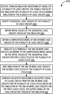
simulate electronically one or more logic circuits of the plurality of logic circuits for first clock cycles of the plurality of clock cycles, the first clock cycles of the plurality of clock cycles corresponding to a second portion of the first waveform;
omit simulation of the one or more logic circuits for second clock cycles of the plurality of clock cycles corresponding to a third portion of the first waveform;
simulate electronically the one or more logic circuits based on the plurality of bits for third clock cycles of the plurality of clock cycles, the third clock cycles of the plurality of clock cycles corresponding to the first portion of the first waveform; and
generate an output waveform of an output signal of a logic circuit from the one or more logic circuits for the plurality of clock cycles based on the simulation of the one or more logic circuits for the first clock cycles and the third clock cycles.
|