| CPC G06F 11/1076 (2013.01) [G06F 3/0619 (2013.01); G06F 3/0625 (2013.01); G06F 3/0644 (2013.01); G06F 3/0673 (2013.01); G06F 11/1048 (2013.01)] | 20 Claims |

|
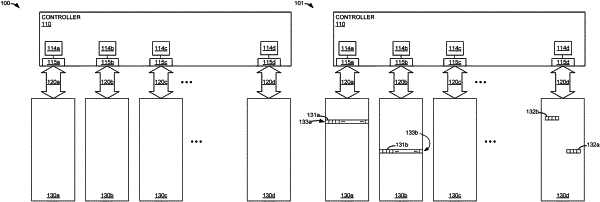
1. A controller, comprising:
at least three of memory channel interfaces that are to operate independently of accesses that occur via the other of the memory channel interfaces;
the memory channel interfaces including an error detection and correction data channel interface, the controller to open a row of a memory device on the error detection and correction data channel interface that is storing a first group of check bits that are associated with a first data word group and a second group of check bits that are associated with a second data word group;
the memory channel interfaces including a first data channel interface and a second data channel interface, the first data channel interface to access the first data word group that is stored contiguously in a first row of a first memory component that is addressed by a first row address and to access a second data word group that is stored in a second row of a second memory component that is accessed via the second data channel interface; and
the controller to receive, from the row of the memory device that is open, the first group of check bits and the second group of check bits.
|