| CPC G06F 1/329 (2013.01) [G11C 5/04 (2013.01); G11C 11/005 (2013.01); H01L 25/162 (2013.01); G06N 20/00 (2019.01); H01L 2224/16146 (2013.01); H01L 2224/16225 (2013.01); H01L 2924/1441 (2013.01)] | 19 Claims |

|
1. An apparatus comprising:
a first logic block including a first circuitry having ferroelectric logic or paraelectric logic;
a second logic block including a second circuitry having CMOS based logic; and
a power management unit having a third circuitry which is coupled to the first circuitry and the second circuitry, wherein the third circuitry is to manage power of the first logic block and the second logic block,
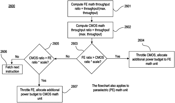
wherein the power management unit is to compute a first throughput ratio of the first logic block, and wherein the power management unit is to compute a second throughput ratio of the second logic block,
wherein the ferroelectric logic or the paraelectric logic includes at least three capacitors with first terminals to receive inputs and second terminals that are directly coupled to a node, wherein at least one capacitor of the at least three capacitors includes non-linear polar material, wherein the ferroelectric logic or the paraelectric logic includes a reset mechanism coupled to the node, wherein the reset mechanism is operable to reset charge on the node in a reset phase separate from an evaluation phase of the inputs, wherein the first logic block and the second logic block have an overlapping functionality, and wherein the power management unit is operable to manage power of the overlapping functionality in the first logic block and the second logic block.
|