| CPC G03F 7/70633 (2013.01) [G03F 7/70625 (2013.01)] | 7 Claims |

|
1. A method, comprising:
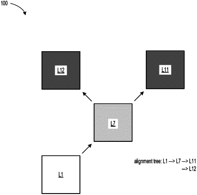
receiving a wafer having a working surface with a first layer and a second layer formed thereon, and a backside surface opposite to the working surface, a target layer to be formed on the working surface that is aligned with the first layer in a first direction and aligned with the second layer in a second direction different from the first direction;
measuring the wafer, with the first layer and the second layer formed on the working surface, to identify a first bow measurement in the first direction;
forming a first stressor film on the backside surface and modifying an internal stress of the first stressor film in the first direction based on the first bow measurement, the first stressor film modifying overlay alignment of the working surface in the first direction across the working surface of the wafer and including no overlay alignment in the second direction across the working surface of the wafer;
forming a first photoresist layer on the working surface that is aligned with the first layer in the first direction;
performing a first lithographic process on the first photoresist layer to form an intermediate hardmask;
measuring the wafer, with the first layer, the second layer and the intermediate hardmask formed on the working surface and the first stressor film formed on the backside surface, to identify a second bow measurement in the second direction;
forming a second stressor film on the backside surface and modifying an internal stress of the second stressor film in the second direction based on the second bow measurement, the second stressor film modifying, overlay alignment of the working surface in the second direction across the working surface of the wafer and including no overlay alignment in the first direction across the working surface of the wafer;
forming a second photoresist layer on the working surface that is aligned with the second layer in the second direction and covers the intermediate hardmask;
performing a second lithographic process on the second photoresist layer and the intermediate hardmask to form a target hardmask; and
performing a target lithographic process on the working surface to form the target layer.
|