| CPC G02F 1/163 (2013.01) [G02F 1/133528 (2013.01); G02F 1/155 (2013.01); G02F 1/157 (2013.01); G09G 3/2007 (2013.01); G09G 3/38 (2013.01); H10K 59/50 (2023.02); G02F 1/137 (2013.01); G02F 2201/44 (2013.01); G02F 2201/52 (2013.01); G09G 2320/0626 (2013.01); G09G 2320/066 (2013.01); G09G 2360/16 (2013.01)] | 11 Claims |
|
1. A display substrate, comprising:
a base substrate;
a plurality of pixel units on the base substrate; and
an electrochromic structure on a side of the plurality of pixel units facing away from the base substrate;
wherein when the display substrate is in a mirror state, transmittance of the electrochromic structure is in an initialization state with a preset value;
when the display substrate is in a display state, the transmittance of the electrochromic structure is positively correlated with brightness of the plurality of pixel units when displaying an image;
the electrochromic structure comprises a plurality of electrochromic units;
the plurality of pixel units are in one-to-one correspondence to the plurality of electrochromic units;
transmittance of each electrochromic unit is positively correlated with brightness of a pixel unit, corresponding to the each electrochromic unit, when displaying the image;
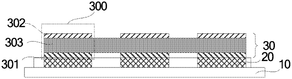
the electrochromic unit comprises: a first electrode and a second electrode arranged sequentially facing away from the base substrate; and an electrochromic film arranged between the first electrode and the second electrode;
the electrochromic film comprises: an ion layer, an electrochromic layer, and an electrolyte layer, arranged sequentially facing away from the base substrate.
|