| CPC G01R 31/3835 (2019.01) [G01R 31/396 (2019.01); H01M 10/48 (2013.01); H01M 10/482 (2013.01); H01M 2220/20 (2013.01)] | 6 Claims |

|
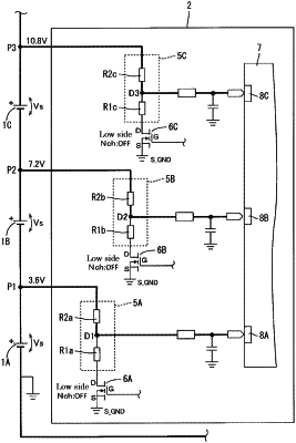
1. A voltage measurement circuit comprising:
voltage dividing circuits that divide voltages of energy storage devices in respective stages connected in series;
switches that cut off currents of the voltage dividing circuits in the respective stages; and
a measurement unit that measures a voltage of each of the energy storage devices in the respective stages based on an output of each of the voltage dividing circuits in the respective stages,
wherein
the voltage dividing circuit in each of the stages includes a first resistor connected to a ground and a second resistor connected to a positive electrode of the corresponding energy storage device,
the switch in a predetermined-number stage among the switches in the respective stages is an N-channel field-effect transistor (FET) having a source connected to the first resistor and a drain connected to the second resistor, and the source of the FET is a voltage output terminal with respect to the measurement unit, and
the switch in a stage, which is a higher stage than the predetermined-number stage where the source of the N-channel FET is connected to the first resistor, is a P-channel FET located on a high side of the voltage dividing circuit.
|