| CPC G01P 15/08 (2013.01) [B81B 7/007 (2013.01); G01P 1/023 (2013.01); G01P 3/00 (2013.01); G01P 15/0802 (2013.01); G01P 15/18 (2013.01); B81B 2201/0228 (2013.01); B81B 2207/012 (2013.01)] | 7 Claims |
|
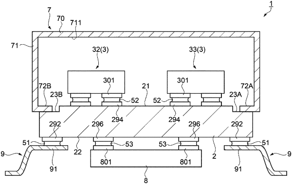
1. A sensor module, comprising:
a substrate, including a first surface and a second surface on front and back sides of each other, an external terminal provided at one of the first surface and the second surface, and an internal terminal provided at the first surface;
a lead bonded to the external terminal and having a gull-wing shape;
a first conductive bonding member having a first melting point and a first Young's modulus, the first conductive bonding member being interposed between the lead and the external terminal, and the first conductive bonding member bonding the lead to the external terminal;
an inertial sensor bonded to the internal terminal, the inertial sensor including a lower surface and a coupling terminal provided at the lower surface, the coupling terminal being configured to input a control signal for controlling the inertial sensor and output a detection signal from the inertial sensor;
a second conductive bonding member having a second melting point lower than the first melting point and a second Young's modulus higher than the first Young's modulus, the second conductive bonding member being interposed between the coupling terminal and the internal terminal, and the second conductive bonding member bonding the coupling terminal to the internal terminal so as to bond the inertial sensor to the internal terminal; and
a cap bonded to the first surface of the substrate so that side walls of the cap, a top plate of the cap extending between distal ends of the side walls, and the first surface of the substrate define an enclosed housing area,
wherein the inertial sensor, the coupling terminal, the internal terminal, and the second conductive bonding member are provided on the first surface of the substrate and disposed within the housing area so as to be housed between the cap and the first surface of the substrate, and
wherein the external terminal, the lead, and the first conductive bonding member are disposed outside of the housing area.
|