| CPC G01J 3/4412 (2013.01) [B81C 1/00206 (2013.01); B82Y 15/00 (2013.01); B82Y 30/00 (2013.01); C23C 18/06 (2013.01); C23C 18/08 (2013.01); G01N 21/658 (2013.01); B81B 2203/0361 (2013.01); B81B 2207/056 (2013.01); B81C 2201/0104 (2013.01)] | 10 Claims |
|
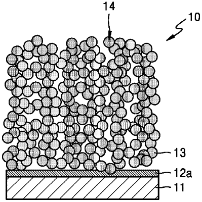
1. A substrate for sensing, comprising:
a support layer;
a seed layer on the support layer;
a plurality of metal nanoparticle clusters arranged on the seed layer, each of the plurality of metal nanoparticle clusters comprising a plurality of conductive metal nanoparticles, and the plurality of conductive metal nanoparticles being stacked in a three-dimensional structure; and
a plurality of perforations arranged among the plurality of metal nanoparticle clusters, wherein each of the plurality of perforations transmits incident light therethrough such that the light excites conductive metal nanoparticles between an upper part of each of the plurality of metal nanoparticle clusters and a lower part of each of the plurality of metal nanoparticle clusters while the light is transmitted along each of the plurality of perforations,
and
wherein a mean size of each perforation from among the plurality of perforations defined by a mean interval between adjacent ones of the plurality of metal nanoparticle clusters is 8 nm to 20 nm.
|