US 12,000,038 B2
Method for manufacturing an electrochemical deposition printhead with grid control circuit and backplane
David Pain, Carlsbad, CA (US); Andrew Edmonds, Oceanside, CA (US); Jeffrey Herman, Solana Beach, CA (US); Charles Pateros, Carlsbad, CA (US); Kareemullah Shaik, San Diego, CA (US); and Edward White, San Diego, CA (US)
Assigned to FABRIC8LABS, INC., San Diego, CA (US)
Filed by FABRIC8LABS, INC., San Diego, CA (US)
Filed on Jul. 12, 2022, as Appl. No. 17/863,272.
Application 17/863,272 is a continuation of application No. 17/099,602, filed on Nov. 16, 2020, granted, now 11,401,603.
Application 17/099,602 is a continuation of application No. 16/926,598, filed on Jul. 10, 2020, granted, now 10,914,000, issued on Feb. 9, 2021.
Application 16/926,598 is a continuation in part of application No. 16/795,495, filed on Feb. 19, 2020, granted, now 10,724,146, issued on Jul. 28, 2020.
Claims priority of provisional application 62/890,815, filed on Aug. 23, 2019.
Prior Publication US 2022/0349046 A1, Nov. 3, 2022
Int. Cl. C23C 16/04 (2006.01); B33Y 30/00 (2015.01); C23C 14/04 (2006.01); C23C 14/08 (2006.01); C23C 14/14 (2006.01); C23C 16/27 (2006.01); C25D 5/10 (2006.01); C25D 17/00 (2006.01); B29C 64/112 (2017.01); B29C 64/209 (2017.01)
CPC C23C 16/042 (2013.01) [B33Y 30/00 (2014.12); C23C 14/042 (2013.01); C23C 14/08 (2013.01); C23C 14/14 (2013.01); C23C 16/278 (2013.01); C25D 5/10 (2013.01); C25D 17/00 (2013.01); B29C 64/112 (2017.08); B29C 64/209 (2017.08)] 20 Claims
OG exemplary drawing
 
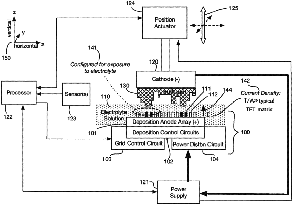
1. A method of making an electrochemical-deposition printhead, the method comprising steps of:
forming deposition anodes by filling openings with a conductive material, the openings extending from a top surface to a bottom surface of a substrate that comprises an insulating material; and
coupling the deposition anodes to a backplane, wherein the backplane comprises:
a grid control circuit, comprising an array of row traces, an array of column traces, a row driver circuit, electrically coupled to the row traces, and a column driver circuit, electrically coupled to the column traces;
a power distribution circuit; and
deposition-control circuits, aligned with a deposition grid, wherein each of the deposition-control circuits is electrically coupled to the power distribution circuit, an associated one of the row traces, and an associated one of the column traces.