| CPC B32B 37/025 (2013.01) [B32B 41/00 (2013.01); B82Y 10/00 (2013.01); B82Y 40/00 (2013.01); H01L 21/762 (2013.01); H01L 29/1606 (2013.01); H01L 29/66045 (2013.01); H01L 29/778 (2013.01)] | 28 Claims |
|
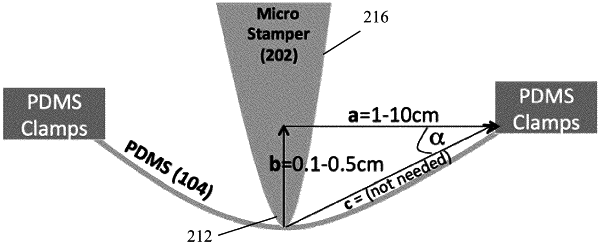
1. A material transfer system for transferring 2-dimensional (2D) material to or from a substrate, said system comprising:
a transfer material comprising an elastic membrane configured to transfer the 2D material, said transfer material having an unpatterned surface;
a holder for supporting the transfer material, said holder permitting the transfer material to stretch;
a transfer micro-stamper having a longitudinal axis that is substantially orthogonal to a plane of the transfer material,
wherein the transfer micro-stamper is configured to move in a stamping direction to stretch the unpatterned surface of the transfer material at a contact point and press the unpatterned surface of the transfer material at the contact point into direct contact with the substrate to thereby transfer the 2D material to or from the substrate.
|