| CPC B23B 27/148 (2013.01) [B23C 5/16 (2013.01); C23C 16/34 (2013.01); C23C 16/36 (2013.01); C23C 16/403 (2013.01); C23C 28/044 (2013.01); B23B 2224/04 (2013.01); B23B 2224/32 (2013.01); B23B 2224/36 (2013.01)] | 12 Claims |
|
1. A cutting tool comprising a substrate and a coating that coats the substrate,
the coating including an α-alumina layer provided on the substrate, the α-alumina layer including crystal grains of α-alumina,
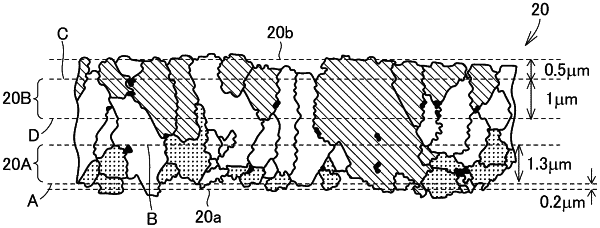
the α-alumina layer including a lower portion and an upper portion,
the lower portion being a region sandwiched between an imaginary plane A and an imaginary plane B, the imaginary plane A being an imaginary plane which passes through a point 0.2 μm away in a direction of thickness from a first interface located on a side of the substrate and is parallel to the first interface, the imaginary plane B being an imaginary plane which passes through a point 1.3 μm further away from the imaginary plane A in the direction of thickness and is parallel to the first interface,
the upper portion being a region sandwiched between an imaginary plane C and an imaginary plane D, the imaginary plane C being an imaginary plane which passes through a point 0.5 μm away in the direction of thickness from a second interface opposite to the side of the substrate and is parallel to the second interface, the imaginary plane D being an imaginary plane which passes through a point 1 μm further away from the imaginary plane C in the direction of thickness and is parallel to the second interface,
the first interface being parallel to the second interface,
when a cross section of the α-alumina layer obtained when cut along a plane including a normal to the second interface is subjected to an electron backscattering diffraction image analysis using a field emission scanning microscope to determine a crystal orientation of each of the crystal grains of α-alumina and a color map is created based thereon,
then, in the color map,
the upper portion being occupied in area at a ratio of 50% or more by crystal grains of α-alumina having a (006) plane with a normal thereto having a direction within ±15° with respect to a direction of the normal to the second interface,
the lower portion being occupied in area at a ratio of 50% or more by crystal grains of α-alumina having a (110) plane with a normal thereto having a direction within ±15° with respect to the direction of the normal to the second interface,
the α-alumina layer having a thickness of 3 μm or more and 20 μm or less.
|