| CPC B08B 3/04 (2013.01) [B08B 13/00 (2013.01); C01B 33/02 (2013.01); C01B 33/021 (2013.01); C01B 33/037 (2013.01)] | 8 Claims |
|
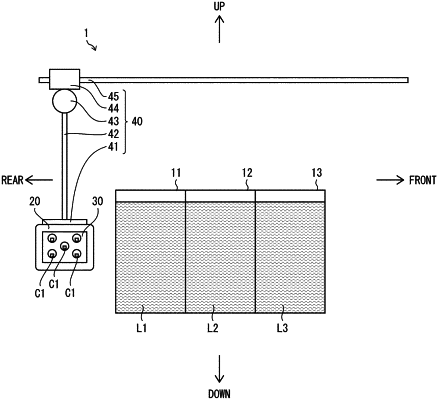
1. A silicon core wire etching device comprising:
an etching bath for holding an etching solution in which a silicon core wire is to be immersed;
a plurality of core wire support members for supporting the silicon core wire, the plurality of core wire support members each having at least one hole, the at least one hole including a hole through which the silicon core wire is to pass; and
a position change mechanism for changing, while the silicon core wire is passed through the plurality of core wire support members and immersed in the etching solution, a relative position where the silicon core wire passes through in relation to the hole.
|