| CPC H05B 33/10 (2013.01) [F21K 9/64 (2016.08); H01L 27/153 (2013.01); H05B 45/00 (2020.01); H05B 45/10 (2020.01); F21K 9/232 (2016.08); H01L 33/0093 (2020.05); H01L 33/08 (2013.01); H01L 33/42 (2013.01); H01L 33/50 (2013.01)] |
| AS A RESULT OF REEXAMINATION, IT HAS BEEN DETERMINED THAT: |
| Claim 3 is cancelled. |
| Claims 1, 2 and 5 are determined to be patentable as amended. |
| Claims 4 and 6-10, dependent on an amended claim, are determined to be patentable. |
|
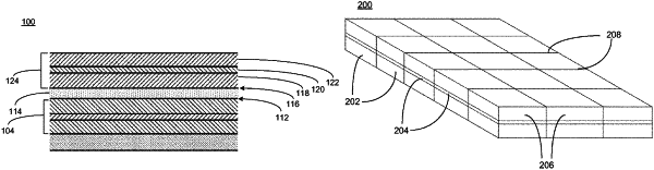
1. A method of fabricating a lighting device comprising the steps of:
providing a substrate having a surface;
forming a substantially planar first LED on the surface of the substrate, the first LED having a surface;
attaching a substantially planar first layer of conductive material on the surface of the first LED, the conductive material having a surface;
forming a substantially planar second LED on the surface of the conductive material;
etching a plurality of troughs through each of the second LED, the first layer of conductive material, [ the substrate, ] and the first LED;
removing the substrate
attaching a color conversion layer to a side surface of at least one of the first LED and the second LED;
wherein the color conversion layer includes an emission latency to reduce or eliminate flicker;
wherein the emission latency of the color conversion layer is asynchronous with polyphase frequencies from a triode AC (triac) power supply;
wherein the polyphase frequencies have a frequency range of up to 240 Hertz;
wherein the first layer of conductive material comprises a transparent conducting film (TCF) chosen from a group consisting of polyethylene terephthalate (PTE), fluorine-doped tin oxide (FTO), carbon nanotube film, graphene film, and poly(3,4-ethylenedioxythiophene) (PEDOT) and its derivatives.]
|
|
2. A method according to claim 1 wherein at least one of first LED
|
|
5. A method according to claim 1 wherein the second LED comprises a surface, further comprising the steps of:
attaching a second layer of conductive material to the surface of the second LED, the second layer of conductive material having a surface; and
forming a third LED on the surface of the second layer of conductive material [ ;
wherein the second layer of conductive material comprises a transparent conducting film (TCF) chosen from a group consisting of polyethylene terephthalate (PTE), fluorine-doped tin oxide (FTO), carbon nanotube film, graphene film, and poly(3,4-ethylenedioxythiophene) (PEDOT) and its derivatives.]
|