| CPC H01L 29/785 (2013.01) [H01L 29/775 (2013.01); H01L 21/823418 (2013.01); H01L 21/823431 (2013.01); H01L 21/845 (2013.01); H01L 27/0886 (2013.01); H01L 27/1211 (2013.01); H01L 29/0673 (2013.01); H01L 29/42392 (2013.01); H01L 29/66439 (2013.01); H01L 29/66795 (2013.01); H01L 29/7848 (2013.01); H01L 29/78696 (2013.01)] | 39 Claims |
|
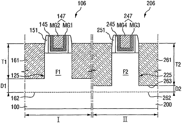
[ 6. An integrated circuit device comprising:
a substrate including a first region and a second region;
a first nanowire shaped transistor disposed on the first region of the substrate, and including a first source/drain; and
a second nanowire shaped transistor disposed on the second region of the substrate, and including a second source/drain, wherein:
the first source/drain has a first thickness, and
the second source/drain has a second thickness that is different from the first thickness, lower surfaces of the first source/drain and the second source/drain being at different heights relative to a bottom of the substrate. ]
|