| CPC H10N 70/063 (2023.02) [H10B 63/82 (2023.02); H10N 70/026 (2023.02); H10N 70/066 (2023.02); H10N 70/841 (2023.02); H10N 70/8833 (2023.02)] | 20 Claims |

|
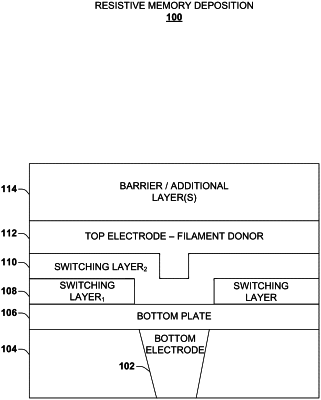
1. A method for fabricating a resistive switching device, comprising:
providing a bottom electrode formed within a dielectric material overlying a substrate of a device;
forming a conductive layer overlying and in contact with both the bottom electrode and the dielectric layer;
forming a first resistive switching layer overlying the conductive layer, wherein the first resistive switching layer is an electrically resistive material;
etching a gap in the first resistive switching layer and exposing a portion of the conductive layer to the gap;
depositing a second resistive switching layer conformally overlying the first resistive switching layer and the portion of the conductive layer exposed by the gap, resulting in a second gap in the second resistive switching layer, wherein the second resistive switching layer is configured to permit diffusion of conductive particles within the second resistive switching layer;
forming a top electrode overlying the second resistive switching layer and filling the second gap, wherein the top electrode comprises the conductive particles and provides the conductive particles for diffusion within the second resistive switching layer in response to an electrical stimulus applied to the resistive switching device;
forming an optional barrier layer overlying the top electrode and a hard mask material overlying the top electrode and optionally the optional barrier layer;
forming and patterning a photoresist overlying the hard mask material; and
etching the hard mask, optional barrier layer, top electrode, second resistive switching layer and the first resistive switching layer, forming a discrete resistive switching device.
|