| CPC H10K 71/233 (2023.02) [H10K 59/1216 (2023.02); H10K 59/124 (2023.02); H10K 71/166 (2023.02); H10K 71/00 (2023.02); H10K 2102/00 (2023.02); H10K 2102/351 (2023.02)] | 21 Claims |
|
1. A method of manufacturing an organic light-emitting display device, the method comprising:
forming a lower electrode pattern on a substrate, which includes a transistor area and a capacitor area, to correspond to the transistor area;
forming a buffer layer on the substrate including the lower electrode pattern;
forming a thin-film transistor including an oxide semiconductor layer on the buffer layer;
forming an interlayer insulating film on the thin-film transistor;
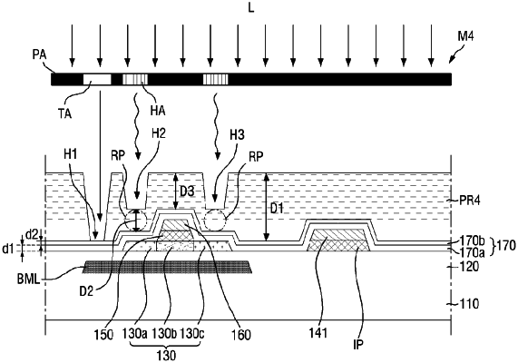
forming a photoresist film pattern including first and second holes, which have different depths, on the interlayer insulating film; and
forming a first contact hole, which exposes the lower electrode pattern, and second contact holes, which expose the oxide semiconductor layer, at the same time using the photoresist film pattern,
wherein the photoresist film pattern includes a residual photoresist disposed between the second holes and the interlayer insulating film,
wherein the interlayer insulating film includes:
a second interlayer insulating film on the buffer layer; and
a first interlayer insulating film between the second interlayer insulating film and the buffer layer, wherein
the first interlayer insulating film is thicker than the second interlayer insulating film.
|