| CPC H10K 59/131 (2023.02) [G02F 1/1343 (2013.01); G02F 1/134309 (2013.01); G02F 1/1345 (2013.01); G02F 1/13452 (2013.01); G02F 1/13458 (2013.01); G02F 1/1357 (2021.01); H10K 59/1213 (2023.02); H10K 59/1201 (2023.02)] | 10 Claims |
|
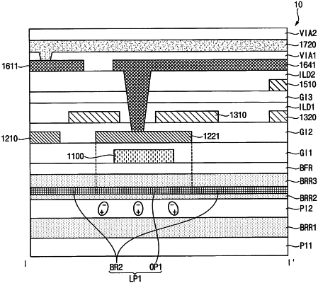
1. A display device comprising:
a substrate including a display area and a non-display area surrounding the display area;
a first lower pattern disposed on the substrate and overlapping the display area;
a second lower pattern disposed in a same layer as the first lower pattern, overlapping the non-display area, and integrally formed with the first lower pattern;
an etch stopper disposed on the second lower pattern;
a power voltage line disposed on the first lower pattern;
a transfer pattern disposed on the etch stopper, connected to the power voltage line, and contacting the second lower pattern through a contact hole defined through the etch stopper; and
a gate electrode disposed on the first lower pattern and disconnected from the first lower pattern,
wherein the power voltage line provides a power voltage, which is a constant voltage, to the transfer pattern, and
the power voltage is provided to the first lower pattern through the transfer pattern and the second lower pattern.
|