| CPC H10K 59/131 (2023.02) [H10K 50/844 (2023.02)] | 11 Claims |

|
1. A display device comprising:
a base substrate;
a thin-film transistor (TFT) layer provided on the base substrate;
a light-emitting element provided on the TFT layer, the light-emitting element being in a display region of the display device;
a frame region provided in a periphery of the display region;
a terminal portion provided at an edge of the frame region extending in one direction;
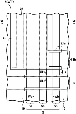
a frame wiring line in the TFT layer, the frame wiring line being provided in the frame region;
a flattening film in the TFT layer, the flattening film being provided in the display region and the frame region, and the flattening film defining a frame-shaped slit in the frame region;
a plurality of first electrodes in the light-emitting element, the plurality of first electrodes being provided on the flattening film;
a second electrode in the light-emitting element, the plurality of first electrodes being between the second electrode and the flattening film, the second electrode interposing a light-emitting layer; and
a conductive layer covering at least an end face of the frame wiring line that is exposed from the frame-shaped slit, the conductive layer and the plurality of first electrode being in a same layer and made of a same material, wherein:
the frame wiring line includes multiple first frame wiring lines,
the first frame wiring line is configured to receives an input of a power supply voltage, and electrically connected to the second electrode,
a pair of the multiple first frame wiring lines respectively reaches either edges of the terminal portion,
the frame wiring line further includes at least one second frame wiring line, and
the at least one second frame wiring line is configured to receive an input of a power supply voltage that has a higher voltage than the power supply voltage received by the first frame wiring, and is electrically connected to a plurality of power source lines disposed in the display region.
|