| CPC H10K 59/124 (2023.02) [H10K 59/122 (2023.02); H10K 77/111 (2023.02); H10K 2102/311 (2023.02)] | 20 Claims |

|
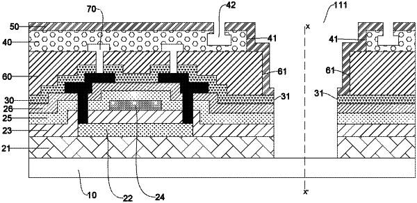
1. A display panel with at least one opening, the display panel comprising:
a substrate;
a thin film transistor structure layer on the substrate;
a first inorganic passivation layer on a side of the thin film transistor structure layer distal to the substrate;
an organic planarization layer on a side of the first inorganic passivation layer distal to the thin film transistor structure layer; and
a second inorganic passivation layer on a side of the organic planarization layer distal to the first inorganic passivation layer,
wherein the at least one opening at least penetrates through the first inorganic passivation layer, the organic planarization layer and the second inorganic passivation layer, and the second inorganic passivation layer extends toward the first inorganic passivation layer along a side of the organic planarization layer proximal to the at least one opening and covers an exposed portion of the organic planarization layer proximal to the at least one opening;
wherein the first inorganic passivation layer has a first sidewall proximal to the at least one opening, and the organic planarization layer has a second sidewall proximal to the at least one opening, and the second sidewall is farther away from a central axis of the at least one opening in a direction perpendicular to the substrate than the first sidewall;
wherein the organic planarization layer comprises a first organic planarization sub-layer and a second organic planarization sub-layer, the first organic planarization sub-layer is on a side of the first inorganic passivation layer distal to the thin film transistor structure layer, the second organic planarization sub-layer is on a side of the first organic planarization sub-layer distal to the first inorganic passivation layer, the first organic planarization sub-layer has a first sub-sidewall proximal to the at least one opening, and the second organic planarization sub-layer has a second sub-sidewall proximal to the at least one opening; and
the display panel further comprises a groove surrounding the at least one opening, wherein the groove penetrates through the second inorganic passivation layer and at least a portion of the second organic planarization sub-layer in the direction perpendicular to the substrate.
|