| CPC H10K 50/86 (2023.02) [G02B 5/3016 (2013.01)] | 20 Claims |

|
1. A phase difference film formed of at least a liquid crystal compound,
wherein an in-plane retardation at a wavelength of 550 nm is 100 to 200 nm,
on a CIE xy chromaticity diagram, Δxy which is a difference between a chromaticity of transmitted light obtained by making light of a standard light source D65 incident on the phase difference film and a chromaticity of the standard light source D65 satisfies Requirement 1, and
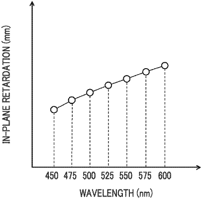
in a graph where wavelengths of measurement light incident on the phase difference film are plotted on a horizontal axis and in-plane retardations of the phase difference film at every 25 nm wavelength of measurement light in a wavelength range of 450 to 600 nm are plotted on a vertical axis, all of slopes S of straight lines connecting two adjacent plot points satisfy Requirement 6,
Requirement 1: Δxy<0.010,
provided that Δxy is calculated by the following formula,
Δxy=((x−x0)2+(y−y0)2)1/2, Formula:
in the formula, x and y represent a chromaticity coordinate of transmitted light of the phase difference film on the CIE xy chromaticity diagram, and x0 and y0 represent a chromaticity coordinate of a standard light source D65 on the CIE xy chromaticity diagram,
Requirement 6: 0.10<Slope S≤1.0.
|