| CPC H10B 41/27 (2023.02) [G11C 5/06 (2013.01); H01L 21/823437 (2013.01); H01L 21/823462 (2013.01); H10B 43/27 (2023.02)] | 19 Claims |

|
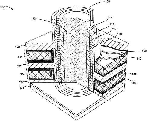
1. A method of forming a memory stack, the method comprising:
depositing a gate metal oxide layer in alternating openings between silicon oxide layers of a memory stack on a substrate having a surface;
preparing a dipole film by exposing the surface of the substrate to a first precursor comprising a dipole metal and optionally to a co-agent comprising nitrogen, oxygen, and/or carbon;
optionally exposing the substrate to a thermal treatment to form the dipole film; and
depositing a metal gate fill layer in the openings, wherein the dipole film is blanket deposited over an entire exposed surface of the gate metal oxide layer, and a subsequent lithography and etch process is used to pattern the dipole film.
|