| CPC H10B 12/30 (2023.02) [H01L 29/41733 (2013.01); H01L 29/45 (2013.01); H01L 29/458 (2013.01); H01L 29/4908 (2013.01); H01L 29/517 (2013.01); H01L 29/6656 (2013.01); H01L 29/66765 (2013.01); H01L 29/66969 (2013.01); H01L 29/78669 (2013.01); H01L 29/78693 (2013.01); H10B 12/05 (2023.02)] | 11 Claims |

|
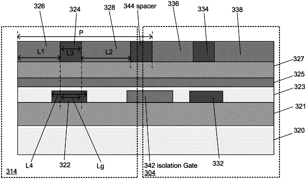
1. A method for forming a thin film transistor (TFT), the method comprising:
forming a gate electrode above a substrate;
forming a gate dielectric layer conformally covering the gate electrode and the substrate;
forming a channel layer above the gate dielectric layer;
forming a source electrode above the channel layer, wherein the source electrode is separated from another source electrode of an adjacent transistor by a pitch, and the source electrode has a first width;
subsequent to forming the source electrode, forming a spacer next to the source electrode and above the channel layer, wherein the spacer has a second width, and overlaps with the gate electrode; and
subsequent to forming the spacer, forming a drain electrode next to the spacer and above the channel layer, wherein the drain electrode has a third width, and wherein a sum of the first width, the second width, and the third width is less than the pitch.
|