| CPC H05K 9/00 (2013.01) | 3 Claims |
|
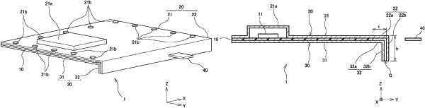
1. An electronic device comprising:
a printed board having first and second opposing surfaces, and an electronic part mounted on the first surface thereof;
a first shield member disposed on and covering the first surface of the printed board, wherein the first shield member has:
a main body portion extending substantially parallel to and in contact with the first surface of the printed board,
a cavity portion that projects away from and out of contact with the first surface of the printed board to form a volume within which the electronic part is disposed, and
a protruding portion that extends beyond contacting one end of the first surface of the printed board as viewed in top plan, by a length (t); and
a second shield member disposed on and covering the second surface of the printed board, wherein the second shield member has a further protruding portion extending beyond contacting the one end of the second surface of the printed board as viewed in top plan, by the length (t),
wherein the protruding portion and the further protruding portion are bent transversely with respect to a plane defined by both the printed circuit board, extend by a length (h) and beyond a side edge of the printed circuit board, and remain separated from one another to form a waveguide through the lengths (t) and (h).
|