| CPC H05F 3/00 (2013.01) [G06F 3/03545 (2013.01); G06F 3/0442 (2019.05); G06F 3/0446 (2019.05)] | 18 Claims |
|
1. An input device for providing input, comprising:
a housing;
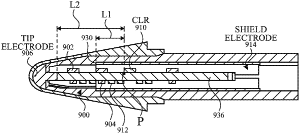
a tip electrode disposed at a tip end of the housing and configured for providing input to a proximate surface;
a handle electrode coupled to the housing;
a plurality of diodes and a current limiting resistance network in a series connection between the tip electrode and the handle electrode, wherein the plurality of diodes includes a first diode and a second diode, the tip electrode is electrically coupled to an anode terminal of the first diode, and a cathode terminal of the second diode is electrically coupled to the handle electrode;
wherein at least one of the plurality of diodes is located between the current limiting resistance network and the handle electrode;
a shield electrode electrically coupled to the handle electrode and substantially surrounding at least a portion of the series connection of the plurality of diodes and the current limiting resistance network, the shield electrode terminating at a shield end located closest to the tip electrode; and
a first pad directly connected to the current limiting resistance network and electrically coupled between the current limiting resistance network and the tip electrode,
wherein a location of the first pad and the current limiting resistance network within the series connection with respect to the handle electrode is selected to produce a total parasitic capacitance between the first pad and the shield and handle electrodes of less than 147 femtofarads.
|