| CPC H04N 25/709 (2023.01) [H04N 25/77 (2023.01)] | 10 Claims |
|
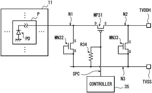
1. A photodetection device, comprising:
a pixel array including a plurality of light-receiving pixels, wherein
each of the plurality of light-receiving pixels includes a light receiver configured to generate an electric charge corresponding to an amount of received light, and
the pixel array is in a first region corresponding to the photodetection device;
a power supply terminal;
a ground terminal;
a switch including a first terminal and a second terminal, wherein
the first terminal is coupled to a first node led to the light receiver,
the second terminal is coupled to a second node led to the power supply terminal,
the switch is configured to couple the first node and the second node by being turned on,
the switch is in a second region corresponding to the photodetection device, and
the second region is outside the first region; and
a first discharge circuit coupled to the first node and a third node led to the ground terminal, the first discharge circuit being configured to discharge electricity from the third node toward the first node.
|