US 11,996,675 B2
Laser drive circuit and sensor apparatus
Mitsushi Tabata, Kanagawa (JP); Takashi Masuda, Kanagawa (JP); Takeshi Yuwaki, Kanagawa (JP); and Toshiyuki Kitazawa, Kanagawa (JP)
Assigned to SONY SEMICONDUCTOR SOLUTIONS CORPORATION, Kanagawa (JP)
Appl. No. 17/250,309
Filed by SONY SEMICONDUCTOR SOLUTIONS CORPORATION, Kanagawa (JP)
PCT Filed Jun. 17, 2019, PCT No. PCT/JP2019/023980
§ 371(c)(1), (2) Date Dec. 31, 2020,
PCT Pub. No. WO2020/012880, PCT Pub. Date Jan. 16, 2020.
Claims priority of application No. 2018-130713 (JP), filed on Jul. 10, 2018; and application No. 2018-130714 (JP), filed on Jul. 10, 2018.
Prior Publication US 2021/0273404 A1, Sep. 2, 2021
Int. Cl. H01S 3/00 (2006.01); H01S 5/042 (2006.01); H01S 5/062 (2006.01)
CPC H01S 5/0428 (2013.01) [H01S 5/042 (2013.01); H01S 5/06226 (2013.01)] 6 Claims
OG exemplary drawing
 
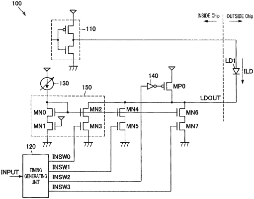
1. A laser drive circuit, comprising:
a first drive current unit configured to adjust, by a first MOSFET and a second MOSFET being connected in series, an inflow of a current to a light-emitting element that emits light in accordance with a current amount when the light-emitting element emits light and when the light-emitting element is extinguished;
a voltage drop unit configured to cause a gate-source voltage of the first MOSFET to drop when the light-emitting element is extinguished; and
a timing generating unit configured to generate a signal for controlling driving of the first drive current unit and the voltage drop unit.