| CPC H01L 33/56 (2013.01) [B29C 33/12 (2013.01); B29D 11/00307 (2013.01); B29D 11/00807 (2013.01); H01L 25/167 (2013.01); B29C 2045/0075 (2013.01); B29C 45/14065 (2013.01); B29C 2045/14114 (2013.01); B29C 45/14639 (2013.01); B29C 2791/006 (2013.01); B29K 2063/00 (2013.01); B29L 2031/34 (2013.01); B29L 2031/3425 (2013.01); H01L 2933/005 (2013.01); H05K 3/284 (2013.01)] | 19 Claims |

|
1. A method comprising:
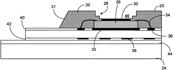
supporting a printed circuit board substrate on a first vacuum injection tool, the printed circuit board substrate having at least one optoelectronic component mounted thereon and having a solder mask on a surface facing away from the first vacuum injection tool;
causing the first vacuum injection tool and a second vacuum injection tool to be brought closer to one another such that a surface of the second vacuum injection tool is in contact with the solder mask; and
subsequently providing a first epoxy, using a vacuum injection technique, in spaces between the second vacuum injection tool and the solder mask;
wherein the printed circuit board substrate covers an area of at least 0.4 times an area of the first vacuum injection tool on which the printed circuit board substrate is supported; and
wherein the printed circuit board substrate and the first vacuum injection tool have an x-dimension and a y-dimension and wherein each of the x-dimension and the y-dimension of the printed circuit board substrate is smaller than a corresponding x-dimension and y-dimension of the first vacuum injection tool.
|