US 11,996,472 B2
Multi-layer dielectric refill for profile control in semiconductor devices
Ya-Yi Tsai, Hsinchu (TW); Chi-Hsiang Chang, Hsinchu (TW); Shih-Yao Lin, New Taipei (TW); Tzu-Chung Wang, Hsinchu (TW); and Shu-Yuan Ku, Zhubei (TW)
Assigned to Taiwan Semiconductor Manufacturing Company Limited, Hsinchu (TW)
Filed by Taiwan Semiconductor Manufacturing Company Limited, Hsinchu (TW)
Filed on Feb. 9, 2023, as Appl. No. 18/166,896.
Application 18/166,896 is a continuation of application No. 17/237,681, filed on Apr. 22, 2021, granted, now 11,600,718.
Prior Publication US 2023/0187542 A1, Jun. 15, 2023
This patent is subject to a terminal disclaimer.
Int. Cl. H01L 29/06 (2006.01); H01L 21/82 (2006.01); H01L 21/8234 (2006.01); H01L 29/417 (2006.01); H01L 29/66 (2006.01); H01L 29/78 (2006.01)
CPC H01L 29/6681 (2013.01) [H01L 21/823431 (2013.01); H01L 29/0649 (2013.01); H01L 29/41791 (2013.01); H01L 29/785 (2013.01)] 20 Claims
OG exemplary drawing
 
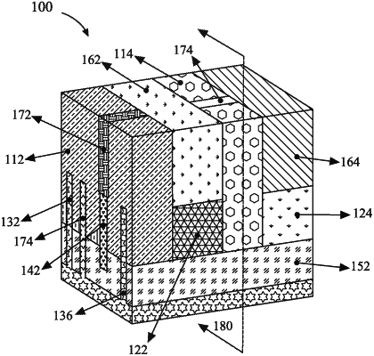
1. A semiconductor device comprising:
an isolation structure;
a fin extending above the isolation structure; and
a dielectric structure formed above the fin, the dielectric structure comprising both a first dielectric layer and a second dielectric layer;
wherein the dielectric structure further comprises a third dielectric layer formed adjacent the second dielectric layer; and
wherein a width of a bottom region of the dielectric structure closest to the fin is greater than a width of a top region of the dielectric structure disposed above the bottom region, and wherein a width of the dielectric structure is less than a width of the fin.