| CPC H01L 29/66234 (2013.01) [H01L 21/22 (2013.01); H01L 29/0649 (2013.01); H01L 29/73 (2013.01)] | 7 Claims |

|
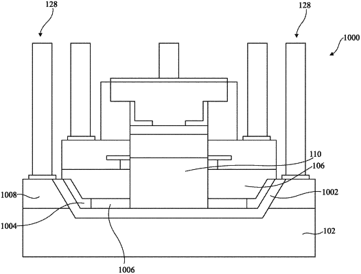
1. A bipolar transistor, comprising:
a semiconductor substrate including a first cavity;
a semiconductor region within the semiconductor substrate along sidewalls and a bottom of the first cavity forming a first portion of a collector for the bipolar transistor;
wherein the semiconductor region is gradually doped, with a doping concentration being highest at the sidewalls and bottom of the first cavity and decreasing with depth into the semiconductor substrate;
a polysilicon layer extending along the sidewalls and a portion of the bottom of the first cavity in contact with the gradually doped semiconductor region of the semiconductor substrate;
an insulating material filling the first cavity to form an insulating trench over the polysilicon layer;
a second cavity extending through the insulating trench to the bottom of the first cavity at the gradually doped semiconductor region of the semiconductor substrate;
a semiconductor material fill in the second cavity forming a second portion of the collector for the bipolar transistor in contact with the first portion of the collector for the bipolar transistor;
a first air pocket located underneath the insulating material filling the first cavity and over the bottom of the first cavity where a part of the polysilicon layer has been removed, said first air pocket located between the semiconductor material fill forming the second portion of the collector and the polysilicon layer extending along the portion of the bottom of the first cavity;
a base region on the semiconductor material fill forming the second portion of the collector; and
an emitter region on the base region.
|