| CPC H01L 29/4236 (2013.01) [H01L 29/401 (2013.01); H01L 29/407 (2013.01); H01L 29/41775 (2013.01); H01L 29/42336 (2013.01); H01L 29/42352 (2013.01); H01L 29/42364 (2013.01); H01L 21/28008 (2013.01); H01L 21/28017 (2013.01); H01L 21/28026 (2013.01); H01L 21/28035 (2013.01)] | 14 Claims |
|
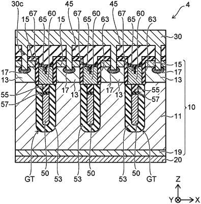
1. A semiconductor device, comprising:
a semiconductor part;
a first electrode provided on a back surface of the semiconductor part;
a second electrode provided on a front surface of the semiconductor part, the semiconductor part having a trench at the front surface side;
a control electrode provided between the first and second electrodes, the control electrode being provided inside the trench of the semiconductor part, the control electrode having top surface facing the second electrode, the control electrode including first and second portions arranged along the top surface side;
a first insulating film provided between the semiconductor part and the control electrode, the control electrode being electrically insulated from the semiconductor part by the first insulating film; and
a second insulating film provided between the second electrode and the control electrode, the second insulating film including a protruding portion extending into the control electrode between the first and second portions of the control electrode, the first and second portions facing each other with the protruding portion interposed, wherein
the semiconductor part includes a first semiconductor layer of a first conductivity type, a second semiconductor layer of a second conductivity type, and a third semiconductor layer of the first conductivity type;
the first semiconductor layer extends between the first electrode and the second electrode, the control electrode being provided between the first semiconductor layer and the second electrode;
the second semiconductor layer is provided between the first semiconductor layer and the second electrode, the second semiconductor layer facing the control electrode via the first insulating film;
the third semiconductor layer is selectively provided between the second semiconductor layer and the second electrode, the third semiconductor layer contacting the first insulating film and being electrically connected to the second electrode;
the protruding portion of the second insulating film has a length in a direction from the first electrode toward the second electrode and a width in a direction from the second semiconductor layer of the semiconductor part toward the control electrode; and the length is greater than the width; and
the length of the protruding portion of the second insulating film is less than a distance from a tip of the protruding portion to a bottom of the control electrode.
|