| CPC H01L 29/4236 (2013.01) [H01L 23/4828 (2013.01); H01L 29/66734 (2013.01); H01L 29/7813 (2013.01)] | 18 Claims |
|
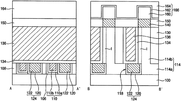
1. A semiconductor device, comprising:
a plurality of semiconductor structures disposed on a substrate,
wherein each of the semiconductor structures includes a first semiconductor pattern that has a linear shape that extends in a first direction and second semiconductor patterns that protrude in a vertical direction from an upper surface of the first semiconductor pattern, wherein the semiconductor structures are spaced apart from each other in a second direction perpendicular to the first direction;
a first conductive pattern formed in a first trench between the first semiconductor patterns, wherein the first conductive pattern extends in the first direction;
a first impurity region formed in the opening in the first semiconductor pattern adjacent to a first sidewall of the second semiconductor pattern, wherein the first impurity region includes an impurity diffusion barrier pattern and a polysilicon pattern doped with impurities;
a gate insulation pattern disposed on the first sidewall of each of the second semiconductor pattern;
a second conductive pattern that extends in the second direction on the gate insulation pattern; and
a second impurity region disposed on each of the second semiconductor patterns,
wherein the impurity diffusion barrier pattern surrounds sidewalls and a bottom of the polysilicon pattern.
|