US 11,996,455 B2
P-type dipole for P-FET
Yongjing Lin, San Jose, CA (US); Karla M Bernal Ramos, San Jose, CA (US); Shih Chung Chen, Cupertino, CA (US); Yixiong Yang, Fremont, CA (US); Lin Dong, San Jose, CA (US); Steven C. H. Hung, Sunnyvale, CA (US); and Srinivas Gandikota, Santa Clara, CA (US)
Assigned to Applied Materials, Inc., Santa Clara, CA (US)
Filed by Applied Materials, Inc., Santa Clara, CA (US)
Filed on Apr. 3, 2023, as Appl. No. 18/130,201.
Application 18/130,201 is a continuation of application No. 17/668,992, filed on Feb. 10, 2022, granted, now 11,658,218.
Application 17/668,992 is a continuation of application No. 17/034,116, filed on Sep. 28, 2020, granted, now 11,289,579, issued on Mar. 29, 2022.
Claims priority of provisional application 63/027,522, filed on May 20, 2020.
Claims priority of provisional application 62/907,668, filed on Sep. 29, 2019.
Prior Publication US 2023/0253466 A1, Aug. 10, 2023
This patent is subject to a terminal disclaimer.
Int. Cl. H01L 29/40 (2006.01); H01L 21/02 (2006.01); H01L 21/28 (2006.01); H01L 29/51 (2006.01); H01L 29/78 (2006.01)
CPC H01L 29/408 (2013.01) [H01L 21/02153 (2013.01); H01L 21/0228 (2013.01); H01L 21/28158 (2013.01); H01L 29/513 (2013.01); H01L 29/517 (2013.01); H01L 29/7851 (2013.01)] 16 Claims
OG exemplary drawing
 
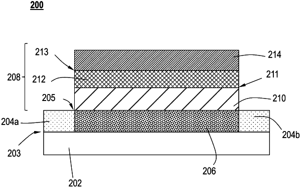
1. A method of manufacturing a p-FET, the method comprising:
depositing an interlayer dielectric on a top surface of a channel located between a source and a drain on a substrate;
depositing a high-κ dielectric material on the interlayer dielectric;
depositing a p-type dipole layer on the high-κ dielectric material, the p-type dipole layer comprising one or more of aluminum nitride and tantalum oxide (TaO);
depositing a capping layer in situ, the capping layer comprising one or more of titanium nitride and titanium aluminum; and
thermally annealing the device.