| CPC H01L 29/1054 (2013.01) [H01L 21/02532 (2013.01); H01L 21/02546 (2013.01); H01L 21/02639 (2013.01); H01L 21/8258 (2013.01); H01L 27/0924 (2013.01); H01L 29/0653 (2013.01); H01L 29/161 (2013.01); H01L 29/20 (2013.01); H01L 29/66522 (2013.01); H01L 29/66545 (2013.01); H01L 29/66795 (2013.01); H01L 29/785 (2013.01)] | 20 Claims |

|
17. A method of forming a field effect transistor (FET) structure, the method comprising:
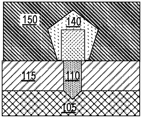
receiving a workpiece including a sub-fin surrounded by isolation dielectric, wherein the sub-fin comprises a first semiconductor material having a first bandgap;
forming a fin wider than the sub-fin by epitaxially growing a second semiconductor material from a portion of the first semiconductor material not covered by the isolation dielectric, wherein the second semiconductor material has a higher carrier mobility than that of silicon and a bandgap narrower than that of the first semiconductor material,
forming source and drain semiconductor material at opposite ends of the fin, and laterally overhanging the isolation dielectric;
forming a gate insulator over a channel region of the fin; and
forming a gate electrode over the gate insulator, wherein a portion of the gate electrode adjacent to a sidewall of the fin is above the isolation dielectric.
|