| CPC H01L 29/0638 (2013.01) [H01L 27/0251 (2013.01); H01L 29/401 (2013.01); H01L 29/41775 (2013.01); H01L 29/42364 (2013.01)] | 20 Claims |
|
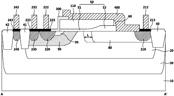
1. A semiconductor device, comprising:
a source region, a drain region, and a gate insulating film formed on a substrate;
a gate electrode formed on the gate insulating film;
a first insulating film pattern formed to extend from the source region to a part of a top surface of the gate electrode;
a spacer formed on a side surface of the gate electrode in a direction of the drain region; and
a second insulating film pattern formed to extend over the gate electrode, the spacer and the drain region,
wherein the second insulating film pattern has a first region formed on the substrate and a second region formed on the gate electrode, and
wherein a length of the first region is less than a length of the second region; wherein the top surface of the gate electrode is formed to be in direct contact with the first insulating film pattern and the second insulating film pattern.
|