| CPC H01L 29/0638 (2013.01) [H01L 21/0245 (2013.01); H01L 29/66545 (2013.01); H01L 29/66795 (2013.01); H01L 29/785 (2013.01)] | 17 Claims |
|
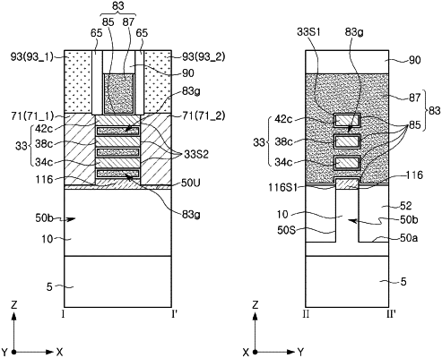
1. A semiconductor device, comprising:
a substrate;
an active region on the substrate;
an isolation region on the substrate and on side surfaces of the active region;
a first source/drain region and a second source/drain region on the active region and spaced apart from each other;
a barrier layer on and contacting the active region;
upper semiconductor layers on the barrier layer and spaced apart from each other in a vertical direction; and
a gate structure covering an upper surface, a lower surface, and side surfaces of each of the upper semiconductor layers in a first direction and extending on the isolation region,
wherein the vertical direction is perpendicular to an upper surface of the substrate,
wherein the first direction is parallel to the upper surface of the substrate,
wherein a material of the barrier layer is different from a material of the upper semiconductor layers,
wherein the barrier layer and the upper semiconductor layers are between the first source/drain region and the second source/drain region,
wherein the barrier layer includes a first side surface contacting the first source/drain region and a second side surface contacting the second source/drain region,
wherein the barrier layer further includes a third side surface and a fourth side surface,
wherein at least a portion of each of the third and fourth side surfaces of the barrier layer contacts the gate structure, and
wherein a lower surface of the gate structure adjacent to the barrier layer is at a higher level than a lower surface of the barrier layer.
|