| CPC H01L 27/15 (2013.01) [H01L 29/7869 (2013.01); H10K 59/12 (2023.02); H10K 59/351 (2023.02); H10K 59/352 (2023.02); H10K 59/353 (2023.02); G09G 3/2003 (2013.01); G09G 3/2074 (2013.01); G09G 3/3208 (2013.01); G09G 2300/0452 (2013.01); H10K 59/121 (2023.02)] | 20 Claims |
|
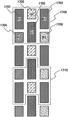
1. A display device comprising:
a first pixel configured to emit light of a first color, the first pixel comprising a first organic EL element and a first color conversion layer provided over the first organic EL element; and
a second pixel configured to emit light of a second color, the second pixel comprising a second organic EL element and a second color conversion layer provided over the second organic EL element,
wherein the first color and the second color are different from each other,
wherein an area of the first pixel is larger than an area of the second pixel,
wherein the first organic EL element is electrically connected to one of a source and a drain of a first transistor,
wherein the other of the source and the drain of the first transistor is electrically connected to a power supply line,
wherein a gate of the first transistor is electrically connected to one of a source and a drain of a second transistor,
wherein the other of the source and the drain of the second transistor is electrically connected to a first signal line,
wherein the second organic EL element is electrically connected to one of a source and a drain of a third transistor,
wherein the other of the source and the drain of the third transistor is electrically connected to the power supply line,
wherein a gate of the third transistor is electrically connected to one of a source and a drain of a fourth transistor,
wherein the other of the source and the drain of the fourth transistor is electrically connected to a second signal line, and
wherein each of the first transistor, the second transistor, the third transistor, and the fourth transistor comprises indium, gallium, and zinc.
|