| CPC H01L 27/14658 (2013.01) [A61B 6/42 (2013.01); A61B 6/44 (2013.01); H01L 27/14603 (2013.01); H04N 25/70 (2023.01)] | 16 Claims |
|
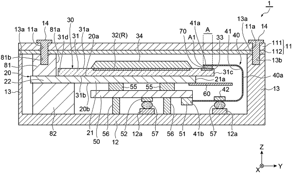
1. A radiation imaging device comprising:
a radiation detection panel having a first surface on which a detection region for detecting radiation is formed and an electrode pad is formed outside the detection region, and a second surface on a side opposite to the first surface;
a base substrate having a support surface configured to face the second surface of the radiation detection panel and configured to support the radiation detection panel;
a flexible circuit substrate comprising:
a first portion which is connected to the electrode pad via a connecting member and
a second portion which is bent to at least partially overlap the first portion when seen in a first direction orthogonal to the support surface and on which an IC chip is mounted; and
a radiation shielding member provided at an edge portion of a back surface of the base substrate opposite to the support surface, wherein a part of the radiation shielding member protrudes to the outside of the base substrate so as to extend between the first portion and the second portion of the flexible circuit substrate and to overlap the IC chip when seen in the first direction,
wherein an end portion of the base substrate is located further inward than an inner end portion of a connection region in which the electrode pad, the connecting member, and the flexible circuit substrate overlap each other when seen in the first direction, and
at least a portion of the IC chip is positioned outside of the end portion of the base substrate when seen in the first direction.
|