| CPC H01L 27/14621 (2013.01) [H01L 27/1464 (2013.01); H01L 27/14643 (2013.01); H01L 27/14831 (2013.01)] | 25 Claims |
|
1. A photodetector comprising:
a semiconductor substrate having an input surface for receiving illumination;
control electrodes for control of photogenerated charge within the substrate; and
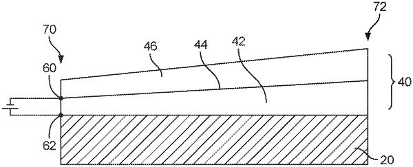
a filter on the input surface of the substrate, the filter comprising a dielectric-metal band pass filter having a metal layer and one or more dielectric layers with one dielectric layer in physical communication with the substrate and the metal layer; and
a connector for applying a bias voltage to the metal layer with respect to the substrate.
|