| CPC H01L 27/1244 (2013.01) [G02F 1/136254 (2021.01); G02F 1/136286 (2013.01); H10K 59/131 (2023.02); H10K 71/70 (2023.02)] | 20 Claims |
|
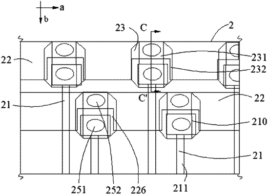
1. A display panel comprising:
a chip-on-film comprising a plurality of first connecting lines arranged in a first direction and spaced apart from each other, wherein the plurality of the first connecting lines extend in a second direction, and the first direction is perpendicular to the second direction; and
a panel body comprising:
a plurality of second connecting lines arranged in the second direction and spaced apart from each other, wherein the plurality of the second connecting lines extend in the first direction;
a first insulation layer arranged between the plurality of the first connecting lines and the plurality of the second connecting lines;
a second insulation layer arranged at a side of the plurality of the second connecting lines away from the plurality of the first connecting lines, wherein the second insulation layer is defined with first holes extending through the first and the second insulation layers, and is defined with second holes extending through the second insulation layer; and
a plurality of third connecting lines arranged at a side of the second insulation layer away from the plurality of the second connecting lines and spaced apart from each other, wherein each of the plurality of the third connecting lines is electrically connected to a corresponding one of the plurality of the first connecting lines via a corresponding one of the first holes, and each of the plurality of the third connecting lines is electrically connected to a corresponding one of the plurality of the second connecting lines via a corresponding one of the second holes;
wherein each of the second holes does not overlap with the plurality of the first connecting lines in a top view.
|