| CPC H01L 27/0255 (2013.01) [H01L 29/0673 (2013.01); H01L 29/66136 (2013.01)] | 11 Claims |
|
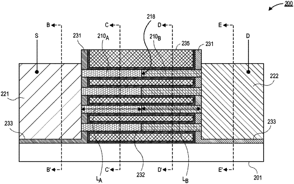
1. A semiconductor device, comprising:
a semiconductor substrate;
a source, the source having a first conductivity type, wherein a first insulator separates the source from the semiconductor substrate;
a drain, the drain having a second conductivity type that is opposite from the first conductivity type, wherein a second insulator separates the drain from the semiconductor substrate; and
a semiconductor body between the source and the drain, wherein the semiconductor body is spaced away from the semiconductor substrate, wherein the semiconductor body comprises a first region adjacent to the source and a second region adjacent to the drain, the first region in physical contact with the second region and wherein the first region has the first conductivity type and the second region has the second conductivity type, and wherein a portion of the first region that has the first conductivity type is in direct physical contact with a portion of the second region that has the second conductivity type.
|
|
9. An electrostatic discharge (ESD) diode, comprising:
a source, wherein the source is a first conductivity type;
a drain, wherein the drain is a second conductivity type that is different than the first conductivity type; and
a plurality of semiconductor bodies between the source and the drain, wherein a depletion region of the ESD diode is along a length of the plurality of semiconductor bodies, wherein the semiconductor bodies comprise a first region adjacent to the source and a second region adjacent to the drain, the first region in physical contact with the second region, and wherein the first region has the first conductivity type and the second region has the second conductivity type, and wherein a portion of the first region that has the first conductivity type is in direct physical contact with a portion of the second region that has the second conductivity type.
|