| CPC H01L 25/167 (2013.01) [G01S 17/04 (2020.01); H01L 21/76898 (2013.01); H01L 23/481 (2013.01); H01L 31/02005 (2013.01); H01L 31/167 (2013.01); H01L 31/1804 (2013.01); H01L 31/186 (2013.01); H01S 5/02325 (2021.01); H04M 1/026 (2013.01); G06F 2203/04105 (2013.01)] | 22 Claims |

|
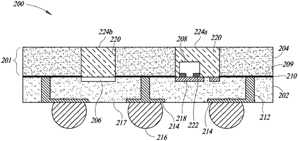
1. A method, comprising:
forming a plurality of light sensors on an upper surface of a silicon substrate;
forming a plurality of contact pads on the upper surface of the silicon substrate;
forming openings in a lower surface of a silicon cap wafer;
aligning the openings with the light sensors and the contact pads;
bonding the silicon cap wafer to the silicon substrate;
removing material from an upper surface of the silicon cap wafer to expose the light sensors and the contact pads;
attaching a plurality of light emitters to respective ones of the contact pads;
thinning the silicon substrate;
filling the openings with a transparent material;
forming through-silicon vias extending from the upper surface of the silicon substrate to a lower surface of the silicon substrate;
forming a ball grid array on the lower surface of the silicon substrate, the ball grid array including a plurality of solder balls electrically connected with respective ones of the through-silicon vias; and
singulating the bonded silicon wafers into individual sensor modules.
|
|
8. A method, comprising:
coupling a cap to a first surface of a substrate including:
overlapping a contact pad at the first surface with a first recess extending into the cap; and
overlapping a light sensor at the first surface with a second recess extending into the cap;
exposing the first recess and the second recess from the cap by removing a portion of the cap extending across and overlapping the first recess and the second recess;
coupling a die to the contact pad in at least one of the following of the first recess and the second recess;
forming a transparent material in the first recess and the second recess;
after coupling the cap to the substrate, forming a first electrical via extending into the substrate at a second surface of the substrate opposite to the first surface, forming the first electrical via includes forming the first electrical via to be in electrical communication with the contact pad; and
after coupling the cap to the substrate, forming a second electrical via extending into the second surface the substrate, forming the second electrical via includes forming the second electrical via to be in electrical communication with the light sensor.
|
|
18. A method, comprising:
coupling a cap to a first surface of a substrate including:
overlapping a first recess in the cap with a contact pad at the first surface of the substrate; and
overlapping a second recess in the cap with a light sensor at the first surface of the substrate;
after coupling the cap to the first surface of the substrate, exposing the first recess and the second recess from the cap by removing a portion of the cap exposing the first recess and the second recess from the cap; and
after coupling the cap to the first surface of the substrate, forming one or more electrical vias extending into a second surface of the substrate opposite to the first surface of the substrate, forming the one or more electrical vias includes forming the one or more electrical vias to be in electrical communication with the contact pad and the light sensor.
|