| CPC H01L 25/167 (2013.01) [H01L 21/6835 (2013.01); H01L 24/95 (2013.01); H01L 2221/68368 (2013.01); H01L 2221/68381 (2013.01); H01L 2224/95001 (2013.01)] | 19 Claims |
|
1. A method of manufacturing a display device, comprising:
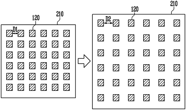
disposing a plurality of light emitting elements on a first transfer film;
stretching the first transfer film so that the plurality of light emitting elements are spaced apart from each other;
transferring the plurality of light emitting elements onto a thin film transistor array substrate; and
removing the first transfer film from the plurality of light emitting elements, wherein
the thin film transistor array substrate comprises a transistor on a substrate, a planarization layer on the transistor, and a first electrode on the planarization layer,
the plurality of light emitting elements are transferred onto the first electrode,
the first electrode is formed on an entire area of a pixel area of the thin film transistor array substrate, and
the transferring occurring absent an alignment of the light emitting elements with elements on the thin film transistor array substrate.
|