| CPC H01L 25/0657 (2013.01) [H01L 2225/06506 (2013.01); H01L 2225/0651 (2013.01); H01L 2225/06562 (2013.01); H01L 2225/06586 (2013.01)] | 11 Claims |
|
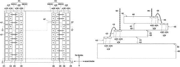
1. A semiconductor package, comprising:
a first chip stack including first and second semiconductor chips which have first side surfaces extending in a first direction, and are offset-stacked toward an opposite side of the first side surfaces of the first and second semiconductor chips to expose edge regions adjacent to the first side surfaces of the first and second semiconductor chips;
a second chip stack formed over the first chip stack and including third and fourth semiconductor chips which have first side surfaces located substantially opposite to the first side surfaces of the first and second semiconductor chips, and are offset-stacked in a direction substantially opposite to an offset stacking direction of the first and second semiconductor chips to expose edge regions adjacent to the first side surfaces of the third and fourth semiconductor chips;
chip pads disposed in each of the edge regions of the first to fourth semiconductor chips, the chip pads including a plurality of first chip pads arranged in a first column along the first direction and a plurality of second chip pads arranged in a second column along the first direction, the first column being closer to the first side surface than the second column in a second direction crossing the first direction, and the first and second chip pads which are adjacent in the second direction being electrically connected to each other;
a first horizontal common interconnector having one end connected to the second chip pad of the first semiconductor chip, and an other end connected to the first chip pad of the second semiconductor chip;
a second horizontal common interconnector having one end connected to the second chip pad of the third semiconductor chips, and an other end connected to the first chip pad of the fourth semiconductor chip;
a first vertical common interconnector having one end connected to the second chip pad of the second semiconductor chip, wherein the second chip pad of the second semiconductor chip is electrically connected to the first chip pad of the second semiconductor chip connected to the first horizontal common interconnector; and
a second vertical common interconnector having one end connected to the second chip pad of the fourth semiconductor chip, wherein the second chip pad of the fourth semiconductor chip is electrically connected to the first chip pad of the fourth semiconductor chip connected to the second horizontal common interconnector.
|