| CPC H01L 24/13 (2013.01) [H01L 23/3121 (2013.01); H01L 24/16 (2013.01); H01L 24/81 (2013.01); H01L 24/97 (2013.01); H01L 2224/13078 (2013.01); H01L 2224/16227 (2013.01); H01L 2224/81815 (2013.01); H01L 2224/97 (2013.01)] | 8 Claims |

|
1. A method for preparing a filter package structure, comprising:
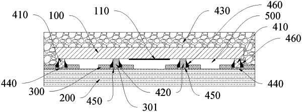
preparing seal walls and support electrodes on a wafer substrate of filters to obtain a finished wafer, wherein the seal walls are respectively disposed around a peripheries of the filters to define enclosed chambers, and the support electrodes are respectively disposed in the enclosed chambers and between the filters and the seal walls;
cutting the finished wafer into a plurality of dies, wherein each of the dies comprises a die substrate, a filter, the seal walls and the support electrodes;
preparing solder layers on electrodes on a substrate, and disposing solder resist layers on peripheries of the solder layer to obtain a finished substrate, wherein a height of the solder resist layers on the substrate is greater than a height of the solder layers on the substrate;
bonding and reflow soldering the plurality of dies to the finished substrate such that the seal walls and the support electrodes are connected to the electrodes on the finished substrate via a solder of the solder layers to obtain a solder structure, wherein in the solder structure, the die substrate, the substrate and the seal walls enclose to define an enclosed chamber, and the support electrodes are disposed in the enclosed chamber; and
disposing a package layer on the solder structure, and cutting the package layer to obtain the filter package structure; wherein
preparing the solder layers on the electrodes on the substrate comprises:
disposing first electrode connection layers and second electrode connection layers on the electrodes on the substrate; and
disposing the solder layers on the first electrode connection layers and the second electrode connection layers;
bonding and reflow soldering the plurality of dies to the finished substrate such that the seal walls and the support electrodes are connected to the electrodes on the finished substrate via the solder of the solder layers to obtain the solder structure comprises:
flipping and placing the plurality of dies on the same finished substrate, and under a first predetermined temperature, causing the seal walls to be pre-bonded to the first electrode connection layers and causing the support electrodes to be pre-bonded to the second electrode connection layers to obtain a pre-assembled structure, wherein in the pre-assembled structure, the die substrate, the substrate, and the seal walls enclose to define the enclosed chambers; and
reflow soldering the pre-assembled structure such that the seal walls and the first electrode connection layers are connected via the solder of the solder layers and the support electrodes and the second electrode connection layers are connected via the solder of the solder layers, and obtaining the solder structure, wherein the solder structure is an assembled structure formed of the plurality of dies and the finished substrate.
|