| CPC H01L 24/08 (2013.01) [H01L 23/3107 (2013.01); H01L 23/49822 (2013.01); H01L 23/49827 (2013.01); H01L 23/49838 (2013.01); H01L 2224/08235 (2013.01)] | 20 Claims |
|
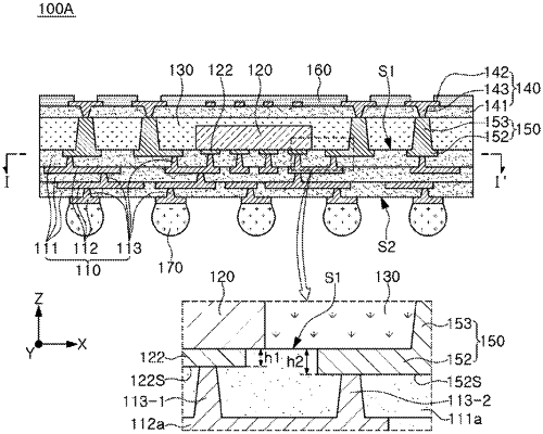
1. A semiconductor package, comprising:
a first redistribution structure that, includes a first insulating layer and a first redistribution layer disposed below the first insulating layer;
a semiconductor chip disposed on the first redistribution structure, wherein the semiconductor chip includes a connection terminal electrically connected to the first redistribution layer and buried in the first insulating layer;
an encapsulant disposed on the first redistribution structure wherein the encapsulant contacts at least side surfaces of the semiconductor chip;
a second redistribution structure disposed on the encapsulant wherein the second redistribution structure includes a second redistribution layer; and
a through via that includes a pattern portion buried in the first insulating layer and electrically connected to the first redistribution layer, and a via portion that penetrates through the encapsulant and electrically connects the pattern portion and the second redistribution layer,
wherein the connection terminal and the pattern portion are located at a first level, and are electrically connected to each other at a second level that is lower than the first level,
wherein the connection terminal has a first side surface,
wherein the pattern portion has a second side surface facing the first side surface of the connection terminal in a first direction, and
wherein the first insulating layer fills between the first side surface and the second side surface in the first direction.
|