| CPC H01L 24/08 (2013.01) [H01L 25/0657 (2013.01); H01L 25/18 (2013.01); H01L 2224/08145 (2013.01); H01L 2924/1431 (2013.01); H01L 2924/14511 (2013.01)] | 20 Claims |
|
1. A semiconductor storage device, comprising:
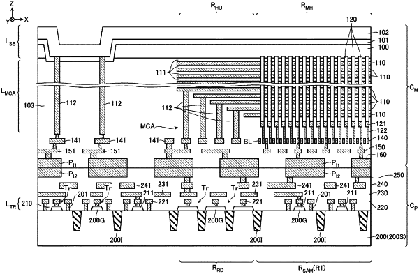
a first chip including a semiconductor substrate, a plurality of transistors, a first interconnect, and a plurality of first bonding electrodes, the first interconnect being at a position between a pair of transistors in the plurality transistors in a first direction parallel to the semiconductor substrate;
a second chip including a memory cell array and a plurality of second bonding electrodes, the second bonding electrodes being bonded to the first bonding electrodes; and
a plurality of bonding pad electrodes on the first chip or the second chip, the bonding pad electrodes being connectable to bonding wires, wherein
the plurality of second bonding electrodes includes:
third bonding electrodes that overlap the memory cell array and are in a current pathway between the memory cell array and the transistors; and
fourth bonding electrodes that overlap the memory cell array but are not in a current pathway between the memory cell array and the transistors,
the first interconnect is electrically connected to a bonding pad electrode in the plurality of bonding pad electrodes,
the first interconnect is not electrically connected to any of the transistors, and
the first interconnect is electrically connected to a fourth bonding electrode in the plurality of fourth bonding electrodes.
|