| CPC H01L 23/5386 (2013.01) [H01L 21/76898 (2013.01); H01L 21/8221 (2013.01); H01L 23/481 (2013.01); H01L 23/5383 (2013.01); H01L 24/09 (2013.01); H01L 24/17 (2013.01); H01L 24/49 (2013.01); H01L 24/73 (2013.01); H01L 27/14621 (2013.01); H01L 27/14627 (2013.01); H01L 27/1463 (2013.01); H01L 27/14634 (2013.01); H01L 27/14636 (2013.01); H01L 27/1464 (2013.01); H01L 2224/73207 (2013.01); H01L 2924/3511 (2013.01); H01L 2924/35121 (2013.01)] | 20 Claims |
|
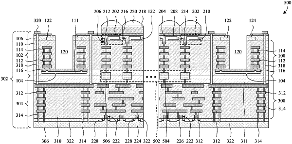
1. A semiconductor structure comprising:
a substrate;
an interconnect dielectric layer underlying the substrate;
a plurality of wires and a plurality of vias alternatingly stacked in the interconnect dielectric layer to define a first conductive column and a second conductive column when viewed in a cross section; and
a pad underlying the first and second conductive columns and directly contacting individual bottom surfaces of the first and second conductive columns respectively at a first interface and a second interface, which have lesser widths than the individual bottom surfaces;
wherein the interconnect dielectric layer has a pair of sidewalls when viewed in the cross section, wherein the pair of sidewalls face each other between the first and second conductive columns and extend from the pad to an elevation above individual top surfaces of the first and second conductive columns.
|