| CPC H01L 23/5385 (2013.01) [H01L 23/5386 (2013.01); H01L 25/0657 (2013.01)] | 20 Claims |
|
1. A semiconductor device, comprising:
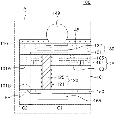
a semiconductor substrate having a first surface and a second surface opposing each other;
a plurality of semiconductor elements disposed on the first surface in a device region, wherein the second surface is divided into a first region overlapping the device region, and a second region surrounding the first region;
an insulating protective layer disposed on the first region of the second surface of the semiconductor substrate, and having an opening region exposing at least a portion of the second region;
an upper insulating layer disposed on the insulating protective layer, and having an extended portion extending onto the at least a portion of the second region in the opening region; and
a connection pad disposed on the insulating protective layer, and electrically connected to the semiconductor elements.
|