| CPC H01L 23/535 (2013.01) [H01L 23/5226 (2013.01); H01L 24/13 (2013.01); H01L 27/0924 (2013.01); H01L 29/0665 (2013.01); H01L 29/41733 (2013.01); H01L 29/41791 (2013.01); H01L 29/42392 (2013.01); H01L 29/78391 (2014.09); H01L 29/7851 (2013.01); H01L 29/78696 (2013.01); H01L 2224/13025 (2013.01)] | 20 Claims |
|
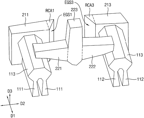
1. An integrated circuit chip comprising:
a substrate;
first channel active regions on the substrate, and extending in a first direction;
second channel active regions on the substrate, and extending in the first direction, the second channel active regions being spaced apart from the first channel regions in a second direction intersecting the first direction;
a first gate electrode and a second gate electrode which intersect the second channel active regions;
a third gate electrode and a fourth gate electrode which intersect the first channel active regions; and
a contact electrode between the first gate electrode and the second gate electrode and between the third gate electrode and the fourth gate electrode, the contact electrode including
a stem section in a vertical direction,
a first branch section extending from the stem section in one direction and contacting a source/drain region on the first channel active regions, and
a second branch section extending from the stem section in the other direction and contacting a source/drain region on the second channel active regions,
wherein the first gate electrode and the third gate electrode overlap with each other in the second direction, and include edge portions having widths decreasing gradually as the first gate electrode and the third gate electrode extend toward facing ends thereof, respectively.
|