| CPC H01L 23/49805 (2013.01) [H01L 21/52 (2013.01); H01L 23/49811 (2013.01); H01L 23/49838 (2013.01)] | 13 Claims |
|
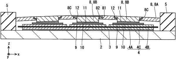
1. A semiconductor device comprising:
a semiconductor element mounted on a circuit pattern provided on an insulating substrate; and
a lead part that has a plate shape and is bonded to the semiconductor element with a first bonding material interposed between the lead part and the semiconductor element, wherein
the lead part includes:
a lead body including an opening part provided corresponding to a mounting position of the semiconductor element; and
a bonding component provided in the opening part and on the semiconductor element, and
the bonding component is bonded at a lower surface of the bonding component to the semiconductor element by the first bonding material and bonded at an outer peripheral part of the bonding component to an inner periphery of the opening part by a second bonding material.
|